Business License
Progressive Stamping for Electronics: A Manufacturer's Guide to Precision Production
Progressive stamping for electronics produces high-volume, tight-tolerance metal parts in one automated pass. Terminals, connectors, shields, and busbars all come off the same die with consistent dimensions. Manufacturers choose this process when they need millions of identical components at a low per-part cost.
What separates an average supplier from a reliable one? In electronics, a single burr, off-pitch terminal, or out-of-spec connector can shut down an assembly line. The right stamping partner combines progressive die stamping expertise, in-house tooling, and a quality system that treats every lot the same, whether the order is 10,000 pieces or 10 million.
In this guide, you will learn how progressive stamping for electronics works, which components it produces, what materials and tolerances matter, and how to evaluate a supplier for your next program. We will also share what Cangzhou Honglang has learned from supplying electrical hardware stamping components to global electronics, automotive, and telecommunications customers.
Key Takeaways
Progressive stamping for electronics produces terminals, connectors, shields, and busbars at high speed with tight pitch control.
In-house progressive die design and manufacturing shortens lead times and protects design confidentiality.
Copper, brass, phosphor bronze, and stainless steel are the most common materials; material choice directly affects conductivity and corrosion resistance.
Tolerances of ±0.05 mm or tighter are common; validation requires in-process inspection, CMM checks, and lot traceability.
Tooling cost is recovered through low per-part cost, making progressive die stamping ideal for medium-to-high-volume programs.
The best partners combine 100+ machine capacity with engineering support, transparent quality processes, and export-ready documentation.
What Is Progressive Stamping for Electronics?

Progressive die stamping feeds a strip or coil of metal through a multi-station die. Each station performs one operation: piercing, blanking, bending, coining, or forming. The part advances from station to station. It is complete when it separates from the carrier strip at the final station.
This process is especially valuable for electronics. It produces complex, small parts with many features in one continuous run. For example, a single terminal may need piercing for contact slots, bending for insertion, and coining for spring force. Progressive stamping performs all of these steps without removing the part from the strip.
As a result, precision metal stamping and progressive die stamping are often the first processes engineers consider for high-volume electronic parts.
The result is a fast, repeatable process well suited to:
High-volume production runs
Tight dimensional tolerances
Complex geometries with multiple bends and forms
Consistent lot-to-lot quality
Low per-part cost after tooling amortization
At Cangzhou Honglang, our electrical hardware stamping components are produced on progressive dies designed and built in-house. That integration lets us tune the strip layout, punch timing, and die clearance for each specific material and part geometry.
Why Electronics Manufacturers Choose Progressive Die Stamping
Electronics manufacturing is unforgiving. A connector that is 0.02 mm out of position may not mate. A shield with a tiny burr can short a circuit board.
Progressive die stamping addresses these risks through speed, precision, and process control. It is the right choice when consistent quality matters more than lowest unit price.
Speed Without Sacrificing Accuracy
A well-built progressive die can run at hundreds of strokes per minute. Each stroke produces a finished part or a finished set of features. That throughput makes high volume stamping the default choice for programs that need tens of thousands to millions of pieces per year.
One Setup, Many Operations
Because the part stays attached to the carrier strip through every station, alignment is maintained from the first pierce to the final bend. This reduces the cumulative tolerance stack that would occur if the same part were moved between separate machines.
Lower Labor Cost per Part
Once the die is installed and qualified, the process runs with minimal operator intervention. Coil feeding, part ejection, and scrap separation can be automated. That efficiency drives down unit cost at volume.
When Li Wei, a procurement manager at a Shenzhen electronics OEM, switched from four single-operation suppliers to one progressive die partner, his team cut inspection reject rates by half. More importantly, his assembly line stopped receiving mixed lots. Every reel of terminals arrived with the same pitch, surface finish, and packaging format.
Want to see how progressive die stamping can simplify your electronics supply chain? Explore our capabilities or send your drawing for a free DFM review.
Common Electronic Components Produced by Progressive Stamping
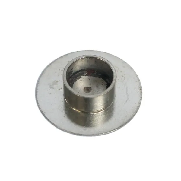
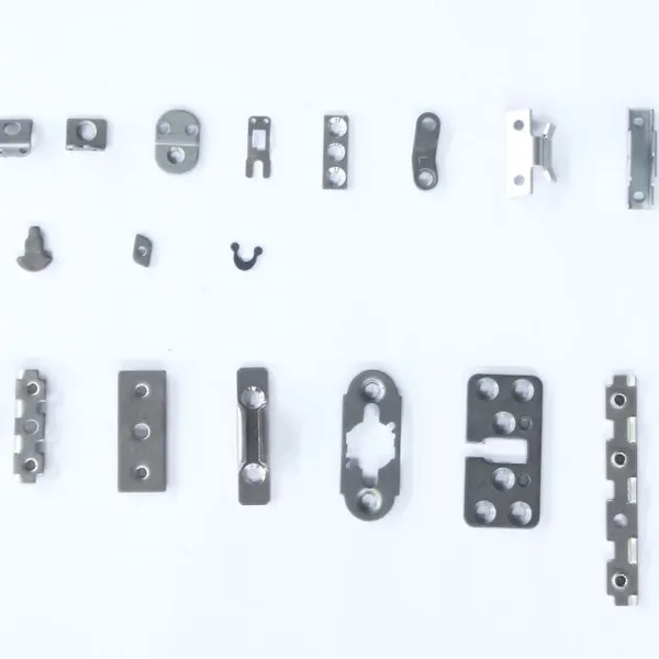
Progressive stamping supports a wide range of electrical hardware stamping components. It is also ideal for custom stamping components with unique geometries, tight pitches, or special finish requirements. The most common electronic parts include:
Terminals and pins, Crimp, solder, and press-fit terminals for wire harnesses and printed circuit boards
Electrical connectors, Multi-cavity housings and contacts with tight pitch requirements
Busbars, Conductive bars for power distribution in EVs, inverters, and telecom equipment
EMI shields and cans, Protective covers that block electromagnetic interference
Heat sinks and clips, Thermal management and retention hardware
Battery contacts and springs, Contacts that require controlled spring force and fatigue life
Lead frames, Metal structures that support semiconductor die attachment and wire bonding
Each of these parts has unique requirements. For example, a terminal may prioritize low contact resistance and clean edges. In contrast, a shield may prioritize flatness and solderability. A lead frame may prioritize etched or stamped features at sub-millimeter pitch.
Cangzhou Honglang supplies components to electronics, automotive, HVAC, and telecommunications markets. Our experience base covers nearly 1,000 product varieties, giving us cross-industry knowledge we apply when reviewing new electronic part designs.
Materials Used in Progressive Stamping for Electronics

Material selection in electronics stamping is driven by conductivity, strength, corrosion resistance, solderability, and cost. Common copper and steel alloys are documented by standards bodies such as ASM International, which publishes authoritative material data for these grades. The most common materials include:
Copper Alloys
C11000 (ETP copper), Highest electrical conductivity; ideal for terminals, busbars, and contacts
C26000 (cartridge brass), Good formability and conductivity; commonly used for connectors and springs
C51000 (phosphor bronze), Excellent spring properties and fatigue resistance; common for contacts and clips
C19400 / C19700 (high-performance copper alloys), Strength and conductivity balanced for miniaturized connectors
Stainless Steel
304 and 316 stainless steel, Used when corrosion resistance or magnetic shielding is required
430 stainless steel, Common for EMI shields due to its magnetic properties
Steel and Nickel Alloys
Cold-rolled steel, Used for structural brackets, clips, and low-cost shields
Nickel silver (CuNiZn), Used for decorative or corrosion-resistant contacts
Surface Finishes
Many electronic parts require plating or coating to improve conductivity, solderability, or environmental resistance. Common finishes include:
Tin plating for solderability
Nickel plating for wear resistance
Silver plating for high-conductivity contacts
Gold plating for critical, low-resistance interfaces
Passivation or chromate conversion for corrosion protection
The right material and finish depend on the end-use environment. For instance, a connector in an outdoor telecom cabinet needs different protection than a terminal inside a consumer appliance. Therefore, Cangzhou Honglang’s engineering team reviews the application, current-carrying requirements, and expected life cycle before recommending a material.
Tolerances, Quality, and Validation for Electronic Stampings
Precision is not optional in electronics. A terminal pitch that is off by 0.05 mm can prevent automated insertion. A connector contact height out of tolerance can create intermittent circuits.
Typical Tolerance Expectations
Dimensional tolerances: ±0.05 mm to ±0.1 mm for most features; tighter when required
Bend angles: ±1° to ±2° depending on material thickness and part geometry
Hole and slot positions: ±0.03 mm to ±0.05 mm for fine-pitch parts
Burr height: Typically less than 10% of material thickness, often tighter for electrical contacts
Quality Processes That Matter
A reliable stamping supplier should offer documentation and processes aligned with electronics industry expectations, including those from organizations such as IPC. Specifically, confirm that the supplier can provide:
In-process inspection with gauges and vision systems
First article inspection (FAI) before production release
Dimensional reports from CMM or optical measurement
Material certificates and lot traceability
Statistical process control (SPC) for high-volume runs
RoHS and REACH compliance documentation where required
Cangzhou Honglang follows the principle of “Quality First, People-Oriented, Customer-Centric, Sustainable Development.” That mindset shapes how we design tooling, set inspection points, and document every production lot. Learn more about our quality and inspection processes.
A telecom OEM once came to us after a previous supplier’s connector lots began drifting out of tolerance midway through a 500,000-piece program. We traced the issue to uneven die wear and a missing in-process check. Our solution included a revised tool-steel selection, scheduled die maintenance, and a station-by-station inspection plan. Lot-to-lot variation dropped to one-third of the previous level.
Tooling Considerations for High-Volume Electronic Parts

Tooling is the foundation of progressive stamping for electronics. A well-designed progressive die can last for millions of cycles, but only if the tooling strategy matches the part complexity, material, and volume. Industry publications such as Metalforming Magazine regularly cover advances in die materials, coatings, and maintenance practices that extend tool life.
Strip Layout and Material Utilization
Engineers design the strip layout to maximize material usage while maintaining part stability through the die. Nesting parts closely reduces scrap but can weaken the carrier strip. The best layouts balance yield, feeding reliability, and tolerance control.
Die Materials and Coatings
For high-volume electronics parts, tool steel selection affects both tool life and part quality. Common choices include:
A2, D2, and M2 tool steels for punches and dies
Carbide inserts for high-wear areas or abrasive materials
PVD coatings such as TiN or TiCN to reduce friction and extend tool life
Progressive vs. Compound Dies
Progressive dies are best for parts with multiple operations and high volumes.
Compound dies combine cutting operations in a single station and can offer better flatness for certain parts but are less flexible for complex forming.
A knowledgeable supplier will recommend the right die strategy based on your part geometry, tolerance requirements, and annual volume.
At Cangzhou Honglang, our engineering team includes 20 technical professionals who handle process analysis, mold design, and mold manufacturing under one roof. That integration means we can adjust tooling quickly when a design changes, rather than waiting for an external die shop.
Cost Factors in Progressive Stamping for Electronics
Understanding cost drivers helps buyers compare quotes and plan budgets. The main cost components in progressive stamping for electronics are:
Tooling Cost
Progressive dies require upfront investment in design, materials, machining, heat treatment, and assembly. Tooling cost varies with part complexity, die size, material, and required tool life. Simple terminals may require a modest die investment; complex multi-cavity connectors require more.
Material Cost
Material is often the largest variable cost per part. Copper and specialty alloys cost more than carbon steel but are necessary for conductivity and corrosion resistance. Material utilization, driven by strip layout, directly affects material cost.
Production Cost
Production cost depends on press speed, die efficiency, labor, inspection, and secondary operations. High-speed progressive stamping lowers per-part cost at volume.
Secondary Operations
Plating, coating, welding, assembly, and packaging add cost but are often required for finished electronic components. A supplier that offers these services in-house or through controlled partners can reduce handling and improve consistency.
The total cost of ownership is what matters. A low unit price from a supplier that requires frequent rework, late deliveries, or external tooling repairs often costs more over the program life than a slightly higher initial quote from a capable, integrated supplier.
If you are comparing quotes for an electronics stamping program, request a detailed quote that breaks out tooling, unit price at multiple volumes, and secondary operation costs.
Choosing a Progressive Stamping Partner for Electronics
Not every stamping supplier is equipped for electronics work. The precision, material sensitivity, and quality documentation requirements demand specific capabilities. Here are six factors to evaluate:
1. In-House Tooling Capability
Suppliers that design and build progressive dies internally can respond faster to engineering changes and protect your intellectual property. They also have deeper control over die maintenance and troubleshooting.
2. Electronics Industry Experience
Ask for samples and case studies from similar applications. A supplier experienced in terminals, connectors, or shields will already understand pitch control, burr management, and packaging requirements.
3. Quality Systems and Documentation
Confirm that the supplier can provide dimensional reports, material certificates, FAI documentation, and RoHS/REACH compliance records. These are often required by electronics OEMs and tier-1 automotive suppliers.
4. Capacity and Scalability
Verify equipment count, facility size, and workforce stability. A supplier with 100+ stamping machines and a large production floor can support both prototype runs and multi-million-piece programs.
5. Secondary Operations
Check whether the supplier offers plating, coating, welding, and assembly. Managing fewer vendors reduces coordination overhead and improves accountability.
6. Communication and Engineering Access
Electronics programs often require quick iteration. Direct access to a technical contact who understands progressive die stamping, materials, and inspection shortens response time and reduces misunderstandings.
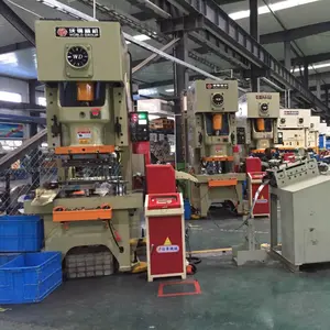
Cangzhou Honglang operates more than 100 sets of stamping machinery across a 10,000-square-meter facility, with 4,000 square meters of built-up production area. Our workforce exceeds 100 people, including 20 technical professionals. We support customers from process analysis and mold design through stamping production, finishing, and export documentation.
An automotive Tier 1 supplier selected Cangzhou Honglang for a new line of stamped battery terminals after a previous partner struggled to hold pitch tolerances across high-volume lots. Our team proposed a revised progressive die layout, added in-line vision inspection, and provided PPAP-ready documentation. The customer reduced incoming inspection sampling and expanded the program to three additional terminals within the first year.
Conclusion

Progressive stamping for electronics is a proven path to high-volume, precision metal components. When the die is engineered correctly, the material is matched to the application, and quality is built into every station, manufacturers receive parts that install reliably, conduct predictably, and withstand real-world use.
The key is choosing a supplier that combines progressive die expertise with in-house tooling, robust quality systems, and the capacity to scale. Price matters, but total cost of ownership, delivery stability, and engineering responsiveness matter more over the life of a program.
If you are planning an electronics stamping project, start by reviewing your drawing with a supplier that understands terminals, connectors, shields, and busbars. Cangzhou Honglang welcomes the opportunity to review your design, recommend materials and finishes, and provide a detailed quote with tooling and volume pricing.
Ready to get started? Request a quote today and receive a free DFM review from our engineering team.
Frequently Asked Questions
What is progressive stamping for electronics?
Progressive stamping for electronics is a metal forming process that produces small, precise electronic components by feeding a metal strip through a multi-station die. Each station performs a cut, bend, or form, and the finished part is separated from the strip at the final station.
What electronic parts are made with progressive die stamping?
Common parts include terminals, pins, connectors, busbars, EMI shields, heat sinks, battery contacts, springs, and lead frames. These parts often require tight tolerances and high-volume production.
What materials work best for electronic stampings?
Copper, brass, phosphor bronze, and high-performance copper alloys are preferred for conductivity and spring properties. Stainless steel and cold-rolled steel are used when strength, corrosion resistance, or magnetic shielding is required.
How tight are tolerances in progressive stamping for electronics?
Typical dimensional tolerances range from ±0.05 mm to ±0.1 mm, with tighter tolerances possible for critical features. Bend angles, hole positions, and burr height are also tightly controlled based on part requirements.
Is progressive die stamping cost-effective for electronics?
Yes, for medium-to-high volumes. The upfront tooling investment is offset by fast production speeds, low labor cost per part, and consistent quality. It is generally not economical for very low volumes or one-off prototypes.
What should I look for in a progressive stamping supplier for electronics?
Look for in-house tooling capability, electronics industry experience, robust quality systems and documentation, scalable capacity, secondary operations support, and direct engineering access.
Recently Posted
-
Metal Stamping Design Guidelines: 7 Rules for Better Parts
August 4, 2026Good metal stamping design guidelines start with matching the part geometry to the right process, material, and tolerance expectat Read More
 -
Stamped Electrical Terminals: A Complete Guide to Materials, Tolerances, and Sourcing
August 4, 2026Stamped electrical terminals are precision-formed metal components that create reliable electrical connections in automotive, elec Read More
 -
Electrical Hardware Stamping Components: A Buyer’s Guide
August 3, 2026Electrical hardware stamping components are precision metal parts made from sheet metal or strip material. They include terminals,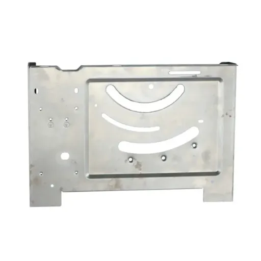 Read More
 -
Sheet Metal Prototyping Services: A Complete Guide for Product Development
August 3, 2026Sheet metal prototyping services help engineers and product teams validate designs, test fit and function, and refine manufacturin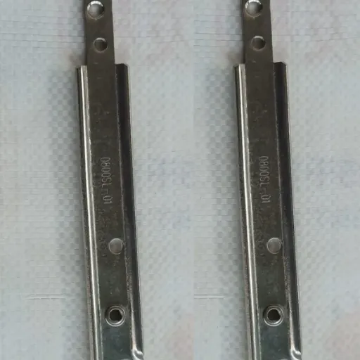 Read More

Contact Us
Recommended Products
-
 Custom Sheet Metal Fabrication: Laser Cutting, Stamping, Bending & Assembly ServicesNegotiableMOQ: 1 Piece
 -
Custom Precision Stainless Steel Metal Stamping Parts for OEM ApplicationsNegotiableMOQ: 1 Piece
-
Custom Automotive Metal Stamping – Stator Rotor Contact Clips for ElectronicsNegotiableMOQ: 1 Piece
-
High-Strength Sheet Metal Stamping for Motorcycle and Automotive ApplicationsNegotiableMOQ: 1 Piece
-
Galvanized Steel Custom Metal Deep Drawing Components Outdoor Deep Drawn Equipment Protective HousingNegotiableMOQ: 1 Piece
-
Professional Sheet Metal Stamping Process Service for Aluminum or Stainless SteelNegotiableMOQ: 1 Piece
-
Customized Stamping Parts for Furniture Auto Electrical Spring ContactsNegotiableMOQ: 1 Piece
-
Precision Custom Metal Deep Drawing Components Custom Sheet Metal Forming Fabrication ServiceNegotiableMOQ: 1 Piece
-
Custom Precision Deep Drawing Stamping Metal Components for IndustryNegotiableMOQ: 1 Piece
-
Stainless Steel Metal Stamping Components - Punching, Bending, Welding ServicesNegotiableMOQ: 1 Piece
-
Custom Deep Drawing Metal Stamping Components for Factory Construction MachineryNegotiableMOQ: 1 Piece
-
Ra0.4 Surface Roughness Metal Stamping Parts for Automotive Brackets PrecisionNegotiableMOQ: 1 Piece
-
Custom Stamping Parts Stamped Welded Deep Drawn Sheet Metal Fabrication ComponentsNegotiableMOQ: 1 Piece
-
Custom Stainless Steel Flat Leaf Spring – Metal Stamping PartsNegotiableMOQ: 1 Piece
-
Custom Sheet Metal Stamping Parts With Bending, Laser Cutting & Fabrication ServicesNegotiableMOQ: 1 Piece
-
Custom CNC Machined Sheet Metal Stamping, Bending, Welding, Laser Cutting & EDM Fabrication ServicesNegotiableMOQ: 1 Piece
-
Custom Precision Metal Stamping Parts High Tolerance Sheet Metal ComponentsNegotiableMOQ: 1 Piece
-
Custom Titanium Sheet Metal Stamping Parts Fabrication for Industrial UseNegotiableMOQ: 1 Piece
-
Durable Custom Metal Deep Drawing Components Surface Treated Forming Components for Construction Engineering EquipmentNegotiableMOQ: 1 Piece
-
China Manufacturer Custom Metal Deep Drawing Components Custom Sheet Metal Deep Drawing FabricationNegotiableMOQ: 1 Piece